

Through hole design is the topic covered this time. This article describes the key points to note when designing through holes, wherein the existing foot patterns of a circuit board for mounting a connector are extended to form through holes.
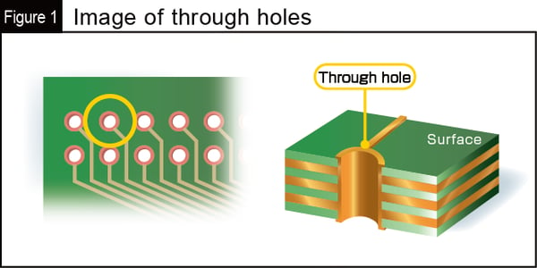
Through holes are bored through a circuit board. They are used for connecting different layers in a multilayer circuit board.
(Figure 1)
Through holes are used to connect the surface and internal wiring of a multilayered printed circuit board, thereby allowing a dramatic increase in the degree of freedom for routing wiring patterns. Moreover, creating through holes on the surface of a multilayer circuit board and probing them allows continuity inspections of the board.
All Panasonic connectors are surface mounts, but not through-hole mounting. However, users may want to form through holes on a circuit board for mounting a connector by extending the existing foot patterns.
(Figure 2)
When applying solder on such an extended trace for mounting the connector, solder may flow along the trace to the through hole. then, a sufficient amount of solder does not remain on the trace for mounting the connector, causing solder mounting defects and poorly soldered joints.
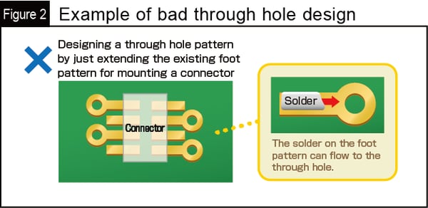
In other words, when just extending the existing foot pattern to form a through hole, it is necessary to devise an effective method to prevent solder from flowing to the through hole for reliable connector mounting.
For this purpose, the following descriptions introduce two typical measures.
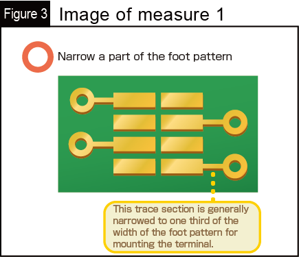
(1) Partly narrow the trace section between the existing foot pattern and through hole (Figure 3):
Partly narrowing the trace restricts the flow of the solder on the connector mounting area to the through hole.
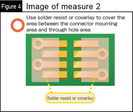
(2) Use a coverlay or resist to cover the area between the terminal mounting area and through hole area (Figure 4):
Coverlay: Sheet that is attached to FPC substrates with adhesives and frequently used for such substrates to protect their surfaces.
Solder resist: Frequently used for rigid circuit boards to protect their surfaces. Solder resist ink is printed on circuit boards.
The coverlay and solder resists are made of materials that prevent solder from flowing (no adhering solder).
By applying these materials to the area between the connector mounting area and through hole area prevents solder from flowing from the connector mounting area to the through hole area.
How did you go with the explanations above? This article summarized the key points to note when forming through holes by extending the existing foot patterns of FPCs. It is important to devise an effective method to prevent solder from flowing from the connector mounting area to the through hole area.
Please make effective use it in this article information when designing through holes.


